SRS Zynq timestamping solution
Introduction to the SRS Zynq timestamping solution
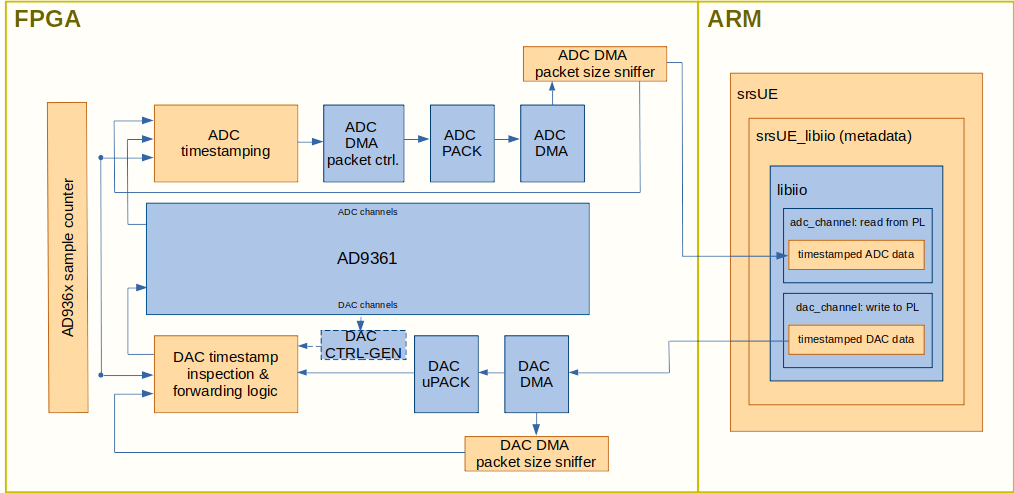
The Zynq timestamping solution provides a sample-aligning mechanism, which is based in counting internal FPGA clock ticks (e.g., in case of reusing ADI's firmware design, the clock-tick counting is derived from the clock signal driving the AD936x chipset; i.e., we are thus counting samples). Based on this sample-counting, SRS solution has the objective of determining the exact clock cycle at which one sample was received from the ADC or needs to hit the DAC interface. The solution is targeting a typical SDR implementation in which the transmission and reception of I/Q samples is triggered by a call to a software function. SRS solution comprises both RTL code and C code and enables exchanging the timestamping information between the CPU and the FPGA as meta-data (i.e., appended to each group of samples written to/read from the related DMA engine). In more detail, from the software side a function call requests a transmission at time instant *N+1ms*, which in the FPGA side will be finally seen as a request to ensure that the samples received through the DMA do arrive at the DAC at a certain timestamp (i.e., clock-count value). In the opposite direction, the FPGA will append a timestamp to each DMA packet (i.e., group of samples forwarded to the CPU). When using AD936x RF chipsets the interfacing to the ADCs/DACs is based on libiio. Then, a libiio wrapper will sit between the high-level software function requesting a reception/transmission of samples and the low-level libiio calls to enable the use of timestamps (as shown in the above diagram). For ZCU111 a custom FPGA and driver implementation is used.